
ASML: Powering The Chip Gold Rush
Building A Moat Around Monopolization

Moore’s Law states that the number of transistors on an integrated circuit doubles roughly every two years. Gordon based this theory on his observations in the late 1950s and early 1960s.

Moore hypothesized that this pace of growth up until the mid-1960s would continue for at least 10 years. And he couldn’t have been more right. This growth rate has stayed true even till today, with the most sophisticated TSMC fabs pushing out 3 nm chips. Apple’s M3 Max is a prime example of a 3nm chipset and has nearly 100 billion transistors packed into one chip.
The bottleneck in maintaining Moore’s law was not even in the hands of TSMC, Samsung, or Intel. In reality, to pack in more transistors in a single chip, there would have to be an evolving technique that made it possible to etch at an increasingly nanoscale. That’s where ASML comes in.
Similar to how newspapers used lithography to create print plates, photolithography was used to etch designs in chips for memory or computing. ASML perfected photolithography, which quickly became the method that offered the highest, throughput, lowest cost, and greatest accuracy.
Photolithography was discovered to be an effective way to etch circuit designs onto a wafer way back in 1950. Silicon wafers were coated with a photoresist, which a light source would then etch to create an integrated circuit. These processes initially used natural light sources visible to the human eye, but challenges arose as the need for smaller chips increased.
ASML had to innovate. By the 1990s, deep ultraviolet (DUV) light allowed chipsets to reduce to 193 nm processes. But DUV was just the start. Extreme ultraviolet (EUV) light, previously thought to be a theoretical concept, was manufactured into reality to enable the single-digit nanometer processes as seen on the Apple M3 Max for example.
However, we aren’t here to discuss the engineering feat at play. I’m surely not the one to be doing that. Moreso answering - is photolithography a defensible business model?
ASML’s Volatile Monopoly
ASML smashed it with photolithography. By the 1990s, the incumbents Nikon and Canon were pushed into obsolescence due to their inability to keep up with the high R&D costs associated with cutting-edge ultraviolet technology. While they still existed in the cheaper areas of the lithography markets, the clear leader was ASML, which controlled 82% of the lithography market. However, their control stretched far past market share.
ASML is still the only manufacturer of these massive photolithography machines made up of over 100,000 components. Unlike the subject of our previous piece, Rivian, ASML orchestrates an intricate horizontal supply chain with over 5,000 suppliers. This leads to them outsourcing over 80% of the finished product.
Given there’s not clear competitor to their EUV product, its safe to say that ASML should continue to maintain its monopoly through the next few decades. However, recent times haven’t been as favorable for ASML. Following an earnings blunder in which the company mistakenly released its guidance a day early, the stock tumbled more than 20% between 2 trading sessions.

The fact is that semiconductors are tricky. While you see the crazy highs that Nvidia or SMCI put up, the industry often sees periods of silence. How often does a company order new $150m semiconductor equipment or update to the latest GPUs? Infrastructure is expensive, and cycles of low sales make it difficult for a company such as ASML to be properly valued in a market that isn’t generally favorable to volatility.
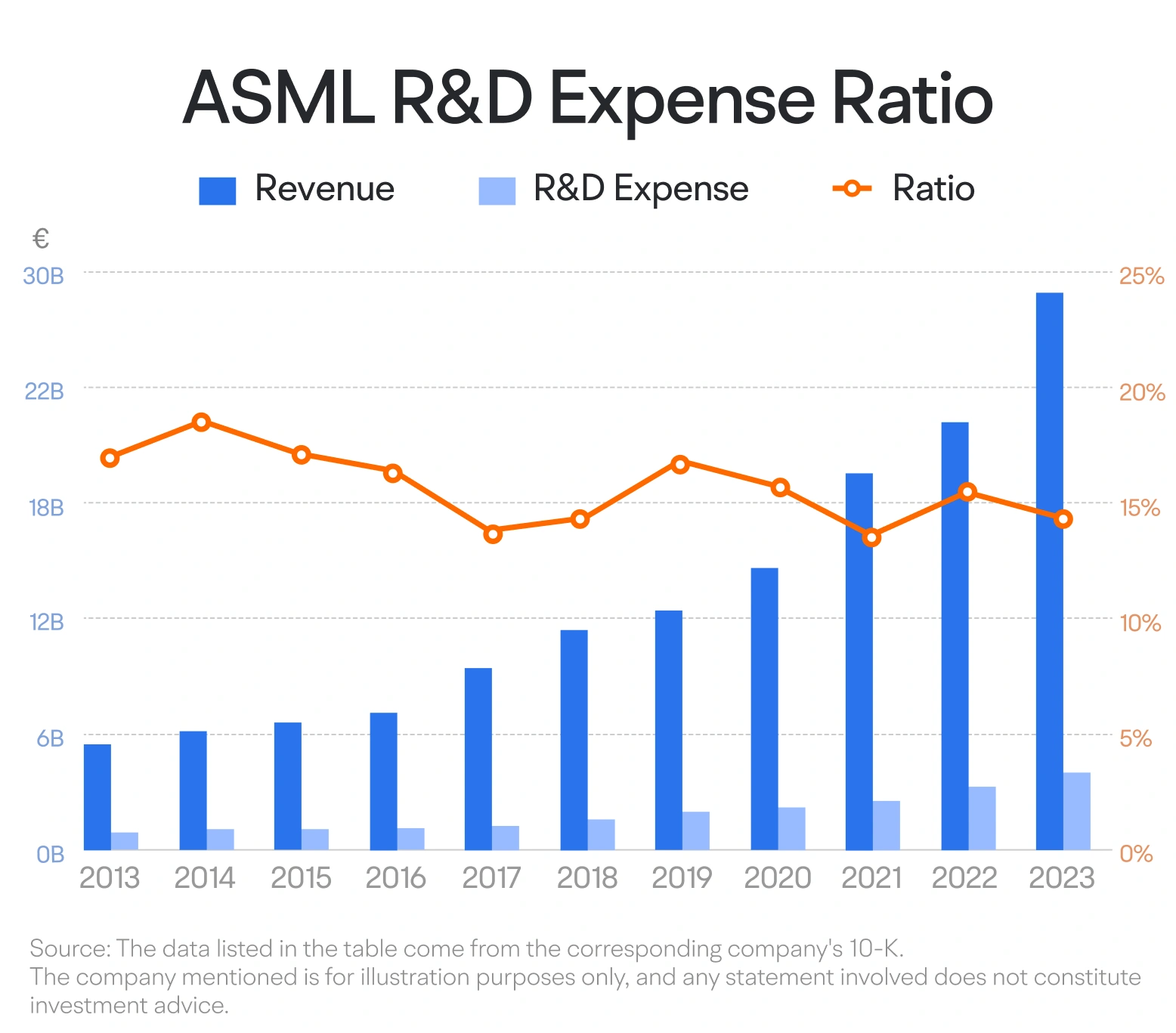
The good news is ASML is always ready to bounce on the next cycle. With a 15% Revenue to R&D expense ratio and almost a 50% expense ratio against net income, ASML is well aware of the investments necessary to keep them at the cutting edge of the manufacturing business. A consistent 15% R&D spend means well more than $3B in R&D over the next few years.
Judging Defensibility
So far we know that ASML’s business model heavily relies on the ability to stay ahead in photolithography. The industry also operates in boom/bust cycles which causes long and silent winters. For context, take a look at the Philidelphia Semiconductor Index (PHLX). $100 bought into the fund between 2001 and 2002 would be worth almost the same 18 years later.

The story of ASML is a story of innovation. The industry innovates beyond imagination when ASML takes something theoretical and turns it into reality (like with EUV lithography). A prime example is the internet bubble and what came after. ASML’s advancements allowed value creation in the form of better computers and mobile phones.
The dot-com bubble isn’t the only example of this. Recent advancements in chip technology coupled with a greater need for data processing enabled the so-called “AI boom”. Nvidia pushed itself to lead the market, TSMC made a name for itself, and ASML, the backbone of the operation, added over $125 billion in value to the company just over the past 4 years.
So when it comes to defensibility, here is the thesis. As long as ASML can innovate in a way that fuels the next wave of innovation (Internet, Cloud, AI, and the next big thing), there are no questions about their moat.
That’s all for today folks! If you enjoyed this piece covering ASML’s domination in the semiconductor manufacturing industry, hit the like button or drop a comment with your thoughts. Simply contact us by replying to this email if you have any insider takes or leave a comment on our Substack page!
A very interesting piece,thanks for putting this together.